
Semiconductors are always changing environments. New technology produces dependable, faster, more efficient equipment. The application of silicon on an insulator wafer marks one of the most fascinating advancements in this domain.
Still, why are these wafers so crucial, and exactly what are they? Let’s examine more closely their features, operation, and advantages for manufacturing and electronics.
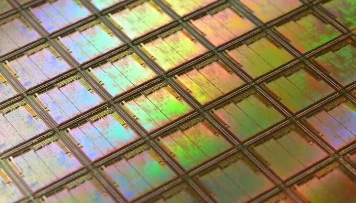
What Is Silicon on Insulator Wafers?
Fundamentally, silicon on insulator wafers are a particular kind of silicon wafer. Silicon wafers are flat, round bits of silicon. Most electrical equipment is built upon them.
Still, one special characteristic of silicon on insulator wafers is their insulating layer. Between two silicon layers rests this layer. It facilitates better performance of electronic equipment.
Usually, silicon oxide makes up the insulating layer. It is quite good at halting the electrical flow. This layer regulates the wafer’s power flow.
Why Do We Need Silicon on Insulator Wafers?
Demand for smaller, more energy-efficient gadgets as well as better ones rises as technology improves. Wafers of silicon on an insulator satisfy these demands. They provide sophisticated electronics with a strong foundation.
From a smartphone to a computer to perhaps a smart home gadget, these devices are enabling the future. Let’s investigate the several ways they contribute.
1. Improving Performance with an Insulating Layer
Performance is much improved in silicon on insulator wafers by the layer acting as insulation. In conventional silicon wafers, electricity occasionally wanders into areas not needed.
This causes interference, which slows down or renders reduced dependability of the gadget. The insulating layer keeps the electricity precisely where it should be, therefore preventing this.
This architecture lets devices more precisely and rapidly handle data. For instance, faster, more dependable processes in a computer depend on silicon on insulator wafers. This implies better performance whether you search the internet, edit movies, or play games.
2. Saving Energy with Lower Power Consumption
Energy efficiency is a key concern in today’s world. Devices such laptops, tablets, and cell phones must run for lengthy stretches without constant charging. By using less power, silicon on insulator wafers helps to reach this. The insulating layer lets electronics run more effectively by lowering the energy waste during operation.
This energy efficiency helps a silicon wafer producer save costs. Reduced energy consumption implies less electricity required to run and manufacture appliances. Larger-scale environmental benefits follow from lower general energy demand, therefore improving the surroundings.
3. Managing Heat Effectively
Operating electronics generates heat. Inappropriate control of this heat could lead to poorer performance or even device damage. By enhancing thermal management, silicon on insulator wafers helps to tackle this problem.
The insulating layer serves as a barrier, therefore stopping too much heat from accumulating. This lets appliances run as they should even with lots of use. A smartphone with silicon on insulator technology, for instance, can manage gaming, video streaming, and other intensive chores without overheating. This increases devices’ dependability and lifetime.
4. Supporting Smaller and More Advanced Devices
Smaller devices with more capability are in increasing demand as technology develops. Consider how skinny cellphones have gotten or how little wearable electronics like smartwatches are now. Miniaturized designs made feasible by silicon on insulator wafers enable this.
These effective wafers cut interference. Manufacturers can thus create smaller circuits without compromising performance. This makes innovative, portable, light-weight, feature-rich products possible.
5. Improving Manufacturing Quality
Making electronic gadgets is a difficult operation; hence, not all wafers become working tools. In manufacturing, a key indicator of efficiency is the success rate, that is, yield. Silicon on insulator wafers lowers production errors, hence improving yield rates.
A more consistent and predictable manufacturing process is created in part by the insulating layer. Less waste of resources and better-quality wafers follow from this. For wafers made of silicon carbide, this translates into fewer expenses and improved goods. For customers, it refers to access to dependable and reasonably priced electronics.
6. Reducing Environmental Impact
In many sectors, including electronics, sustainability is starting to take front stage. Environmental impact-wise, silicon on insulator wafers are better. To make them requires less energy and less raw materials.
Given the global search for methods to cut waste and save resources, this decreased environmental impact is significant. Choosing silicon on insulator technology allows producers to satisfy modern technology needs while nevertheless helping to create a better future.
7. Enabling Advanced Technologies
The rise of advanced technologies like the IoT and AI depends on efficient, powerful semiconductors. Silicon on insulator wafers is exactly fit for these needs.
They help to control heat, conserve energy, and improve performance. They thus are perfect for smart devices, linked houses, and automated systems. Big data sets have to be handled fast in artificial intelligence applications.
8. Adopting This Technology
Clear advantages of silicon on insulator wafers exist. All the while helping the creation of innovative technologies, they provide better performance, energy savings, and environmental advantages. To keep competitive in the always-changing electronics sector, several manufacturers are switching from conventional silicon wafers to silicon on insulator wafers.
Using this technology will help businesses design products that satisfy the needs of contemporary consumers and also become ready for next developments.
Silicon on insulator wafers is helping to shape electronics going forward. They are in wearable fitness trackers, high-performance computers, and creative artificial intelligence systems. Consider exploring more about patterned wafers and how they might benefit your next manufacturing project.
The Future of Silicon on Insulator Wafers
The function of silicon on insulator wafers will become even more important as the semiconductor sector keeps expanding. Modern electronics are based mostly on their capacity to handle issues including energy efficiency, thermal control, and downsizing.
Scientists and engineers are always researching methods to make these wafers even better in this domain. The opportunities are limitless, from refining their design to discovering fresh uses. One thing is definite: silicon on insulator wafers is here to stay and their influence on technology will only keep increasing.
A Step Towards Smarter Electronics Using Silicon on Insulator Wafer
Looking ahead, the value of silicon on an insulator wafer will just grow. This technology marks a path towards smarter, more sustainable electronics for consumers and producers equally. Silicon on insulator wafers are worth keeping an eye on whether your next great tech invention is under development or you just want to know what semiconductors might hold going forward.
Drain Cleaning Business: Clearing the Path to a Healthy Home


Comments